Jijun Huang(黄及军) and Xueling Lei(雷雪玲)
Department of Physics,Jiangxi Normal University,Nanchang 330022,China
Keywords: point defects,MgS semiconductor,qubits,first-principles calculations
The defects of wide-bandgap semiconductors have attracted extensive attention due to their great potential for applications in quantum sensing,[1,2]information processing,[3,4]and so on. For example, point defects in semiconductors are used as quantum sensors to measure temperature,[5,6]electric field,[7]magnetic field,[8]etc. It is known that the famous negatively charged NV color center and SiV color center in diamond[9–11]have excellent properties,e.g.,microwave manipulation,[12]long spin coherence time,[13]and controllable coupling between individual electronic and nuclear spins.[4]However,the preparation process of NV-color center in diamond is still challenging because of the requirements of high concentration and controllable position.[14–16]Therefore, it is necessary to find other potential qubits to apply in the quantum systems. So far,many candidates have been proposed,such as negatively charged Si vacancy(V-Si),[17,18]neutral carbon–silicon double vacancy (VCVSi),[19,20]and negatively charged NV color center(NCV-Si)[21]in SiC,the neutral VAlONin wurtzite AlN,[22]the neutral VGaONin GaN,[23]etc.
MgS is a typical wide-bandgap semiconductor (experimental bandgap: 4.45 eV[24,25]) with diamond like structure,and it has been successfully prepared experimentally. Inspired by the above works, the phosphorus-doping defect (PS) in MgS as a potential qubit has been systematically investigated using first-principles calculations. The aim of this work is to find a qubit candidate with excellent quantum properties. The formation energy,defect levels,and electronic structure of the PSdefect in different charge states are evaluated. The zerophonon line (ZPL) and zero field splitting (ZFS) of neutral P0Sand positively charged P+1Sare discussed, and the hyperfine tensors are examined. Our calculations suggest that the neutral P0Sand positively charged P+1Sare the plausible qubit candidates for the construction of quantum systems.
All the first-principles calculations in this work have been carried out using the Viennaab initiosimulation package(VASP)[26,27]in the framework of the density functional theory (DFT). The interaction between core ions and valence electrons was described by the projector augmented wave(PAW) method[28,29]and the generalized gradient approximation (GGA) parametrized by Perdew–Burke–Ernzerhof(PBE)[30]was used for the exchange–correlation functional.Geometries of the 2×2×2 MgS supercell with one Ps defect in different charge states were fully optimized using a plane wave cutoff of 400 eV without any symmetry restrictions,the energy and force convergence were set to be 1×10⁻⁵eV and 0.01 eV·˚A-1, respectively. The 0.02 ˚A-1Monkhorst–Packk-point density of the supercell was set for Brillouin zone sampling.[31]It is known that the bandgap calculated with PBE usually has been underestimated, and the Heyd–Scuseria–Ernzerhof (HSE06)[32,33]hybrid exchange–correlation functional allows one to solve this problem. Then the HSE06 was afterward chosen to study the electronic structures and optical properties.
In order to describe the stability of the P-doped point defects(denoted as PS), the defect formation energy was calculated according to[34]
3.1. Structural and electronic properties of the PS point defects in MgS
The optimized structure parameters and bandgap of MgS primitive cell are listed in Table 1,from which we can see that
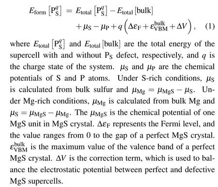
the lattice parameter of MgS primitive cell is 4.025 ˚A and the Mg–S bond length is 2.465 ˚A.The point defect of PShas been created by substituting one P atom for one S atom in a 2×2×2 MgS supercell. Since each S atom in MgS is equivalent,there is only one type of the PSpoint defect. The optimized geometry of the neutral PSpoint defect along with the electronic structures is shown in Fig.1. After optimization,the PSpoint defect hasC3vsymmetry. As shown in Fig.1(a),the distances between P atom and the four nearest Mg atoms are 2.51 ˚A,2.51 ˚A,2.51 ˚A,and 2.68 ˚A,respectively. Comparing with the distance of S–Mg in the perfect MgS crystal(2.47 ˚A),all the distances of P–Mg have been stretched. Mg4and P atoms are on the axis of symmetry. The distance of Mg4–Mgi(i=1,2, 3) is 4.10 ˚A, and the distance between Mgi(i=1, 2, 3)is 4.20 ˚A.According to formula(1),the calculated formation energy of the neutral PSpoint defect (q=0) is 4.10 eV and 0.54 eV under S-rich and Mg-rich conditions,respectively,indicating that the PSpoint defect is easy to form in the case of Mg-rich.
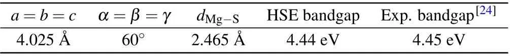
Table 1. The structure parameters and bandgap of the MgS primitive cell.
Fig.1.The schematic diagram of the PS point defect in a 2×2×2 MgS supercell and the local structure of the PS point defect(a)and corresponding projected density of states(PDOS)(b),the amplified PDOS(c)and band structure(d)with an energy range of-1.00 eV to 1.00 eV.
Now, we turn to examine the electronic structures of the PSpoint defect. The electronic structures calculated from 4×4×4 supercell with 512 atoms are presented in Fig. S1 in the supplementary material,from which the characteristics of electronic structures are the same as those of 64 atoms supercell. As shown in Fig.1(b),the spin polarization projected density of states (PDOS) of the PSpoint defect shows that there are six defect states due to introduction of the impurity P atom. Of those defect states, two occupied defect states lie very deep in the valence band,one is spin-up electronic state at-8.67 eV,the other is spin-down electronic state at-8.02 eV,so the two states play no important role in the excitation or ionization processes.Four defect states are located in the bandgap of the host material MgS.Of those,three defect states are occupied electronic states and the remaining one is the unoccupied electronic state. Further observation, it is found that the peak of two occupied states close to the Fermi level is about twice as high as that of one occupied state near the valence band maximum (VBM), indicating that the two occupied defect states are double degenerate states. To illustrate this, we further examine the band structure near the Fermi level. Figure 1(c) shows the amplified band structure with an energy range of-1.00 eV to 1.00 eV. We note that there are indeed two double degenerate defect levels below the Fermi level,one is spin up and the other is spin down. And there are two singlet defect levels in the gap of the MgS, one is close to the VBM and the other one is above the Fermi level, this is consistent with the results in Fig.1(b). Combined with the PDOS and the amplified band structure,it is easy to know that there are five defect energy levels occupied by electrons,and two of them are double degenerate defect energy levels. As a result,the defect energy levels have been occupied by seven electrons. However,the impurity P atom has a total of five valence electrons,so where do the extra two electrons that occupy the defect energy levels come from? To understand this question,we further draw the amplified PDOS near the Fermi level, as shown in Fig. 1(d), from which we can see that the occupied electronic states in the gap are mainly from the contributions of the valence electrons of P atom and S atom, and slightly from the contributions of Mg atom. Therefore,the defect energy levels are mainly occupied by five valence electrons of P atom and two valence electrons of S atom.
To confirm the above results, we further plotted the schematic diagram of the defect energy level sequence and the corresponding partial charge densities,as shown in Fig.2.According to the molecular orbitals(MOs)theory in the system withC3vsymmetry,[35]there are two non-degenerate MOs a1(1)and a1(2)in the one-dimensional irreducible representation (IR) ofA1space and two degenerate MOsexandeyin the two-dimensional IR ofEspace. Correspondingly, there are two non-degenerate levelsE1andE2,and two degenerate levelsExandEy,i.e.,theE1,E2andExylevels. Based on the analysis of electronic structures, the defect energy levels of the PSpoint defect from high to low are as follows:E↓1,E↓xy,E↑xy,E↑1,E↓2,E↑2, whereExyrepresents double degenerate defect levels. According to Fig.2(a),the defect energy levels are occupied by seven electrons. Specifically,theE2andExylevels are fully occupied by six electrons,and theE1levels is half occupied (spin up) by one electron. Therefore, the net spin of the system isS=1/2 and then the system is spin-doublet.As seen in Fig.2(b),the P atom and its nearest S atoms make the largest contribution to the charge density of theE1andExylevels, while the charge density of theE2level is only localized on the P atom, showing that theE2is occupied only by the valence electrons of P atom. Considering the distribution shape of the electron density, it can be concluded that the 3p electrons of P atom and S atom occupy theE1andExylevels,and 3s electrons of P atom occupy theE2level. Furthermore,we also observe that the area of charge density distributed onExyis almost twice as large as that distributed onE1,indicating that theExylevel is a double degenerate energy level. These results are in good agreement with the aforementioned electronic structure analysis.Table 2. Energies(in eV)of the P0Sdefect levels(E↓1andE↓xy),CBM,VBM,and the energy gap(ΔE,ΔEcand ΔEV)calculated by HSE06 and PBE,respectively.The energies ofE↓1,E↓xy,CBM and VBM are relative to the Fermi level,and the Fermi level is set to be zero.
Fig. 2. The schematic diagram of the defect energy levels (a) and the partial charge density of molecular orbitals (b) in the PS defect in the order of energy from high to low. The isosurface value is 2×10⁻³ e/˚A3. The black arrow indicates the position of the PS defect.

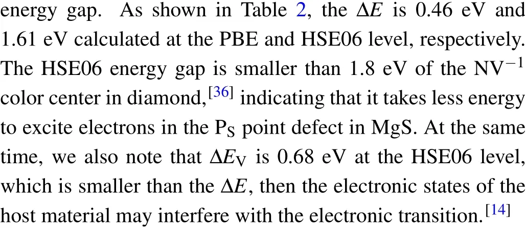
E↓1 E↓xy CBM VBM ΔE ΔEc ΔEV PBE 0.23 –0.23 2.50 –0.88 0.46 2.27 0.65 HSE06 1.17 –0. 44 3.35 –1.12 1.61 2.18 0.68
3.2. Different charge states of the PS point defects in MgS
As aforementioned, the total spin of the neutral PSpoint defect isS=1/2 with one unpaired electron, whereSis the spin angular momenta, and then the neutral PSpoint defect is spin-doublet. As we know, the triplet qubit with total spinS=1 can be easily manipulated by microwave(MW),so the properties of the PSpoint defect in different charge states have been investigated to find easily manipulated triplet qubit. First of all,the energetic stability of the PSpoint defects in different charge states was evaluated using the formation energy calculated via formula(1). Figure 3 shows the formation energy of the PSpoint defects in the charge stateq(q=-1, 1, 2) as a function of the Fermi level,where each line represents the formation energy for a specific charge state,and the slope represents the charge state of the system.Obviously,the most stable charge state is affected by the position of the Fermi level,e.g.,the solid black lines represent the most stable charge state of the PSdefect with the lowest formation energies corresponding to different Fermi levels. The neutral PSpoint defect is stable forεF=1.96–2.60 eV. With the Fermi level varying from the VBM to CBM, the most stable charge state of the PSpoint defect exhibits P+2S,P+1S,P0Sand P-1S,with transition of+2/+1, +1/0 and 0/-1. The values of the corresponding charge transition level are 1.51 eV, 1.96 eV and 2.60 eV,respectively.
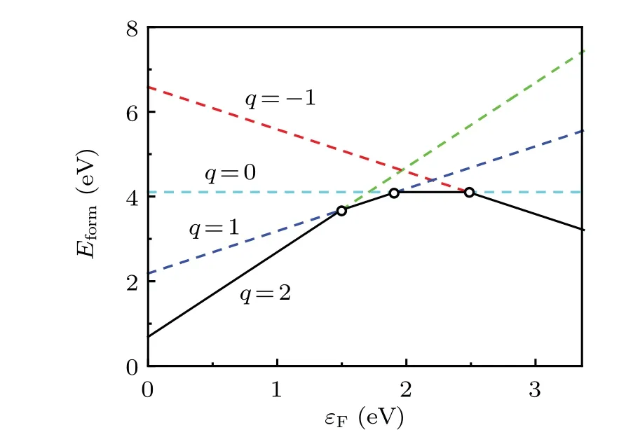
Fig. 3. Formation energies (Eform) of the PS point defect in different charge states as a function of Fermi level(εF),the slope represents the charge state q.
Then the basic electronic properties of the PSpoint defects in different charge states were calculated and shown in Fig.4.
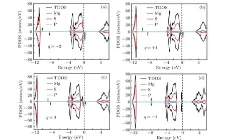
Fig.4. The projected density of states(PDOS)of the PS point defect in different charge states.

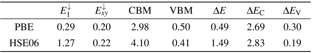
Table 3. Energies(in eV)of the P+1S point defect levels(E↓1 and E↓xy),CBM,VBM, and the energy gap (ΔE, ΔEc and ΔEV) calculated by HSE06 and PBE,respectively. The energies of E↓1,E↓xy,CBM and VBM are relative to the Fermi level,and the Fermi level is set to be zero.
3.3. Optical properties of the P0S and P+S 1point defects in MgS

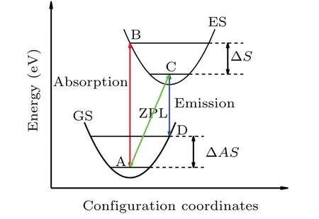
Fig. 5. The schematic diagram of the configuration coordinate of PS’ground state and excited state. The red and blue arrows represent vertical absorption and vertical emission, respectively, and the green arrow is the zero-phonon line (ZPL). ΔS and ΔAS stand for Stokes shift and anti-Stokes shift,respectively.
Table 4. The zero-phonon lines(in eV)of the PS point defect in various charge states calculated at the HSE06 level.

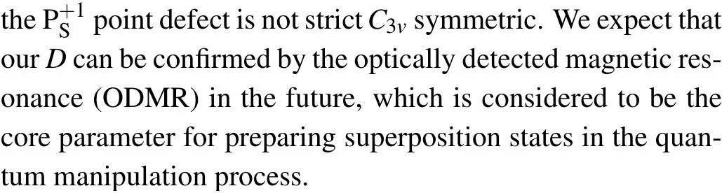
As a result,D=2920 MHz andE=-265 MHz. The value ofDis obviously in the range of MW,and in fair agreement with the theoretical data 2980 MHz of the VBONcenter in c-BN crystal.[16]However,the value ofEis ten orders of magnitude smaller thanD.We note that theEis not zero,perhaps because
3.4. Hyperfine parameters of the P0S and P+S1 point defects in MgS
The hyperfine tensor reflects the interaction between nuclear spin and electron spin.[38]As we know,although the nuclear spins of24Mg and32S are zero, the25Mg (with natural abundance of 10.11%),33S(0.75%)and31P(100%) have nonzero nuclear spins of 5/2,3/2,and 1/2,respectively.Therefore, the hyperfine tensors have been calculated in this work,which are expressed as
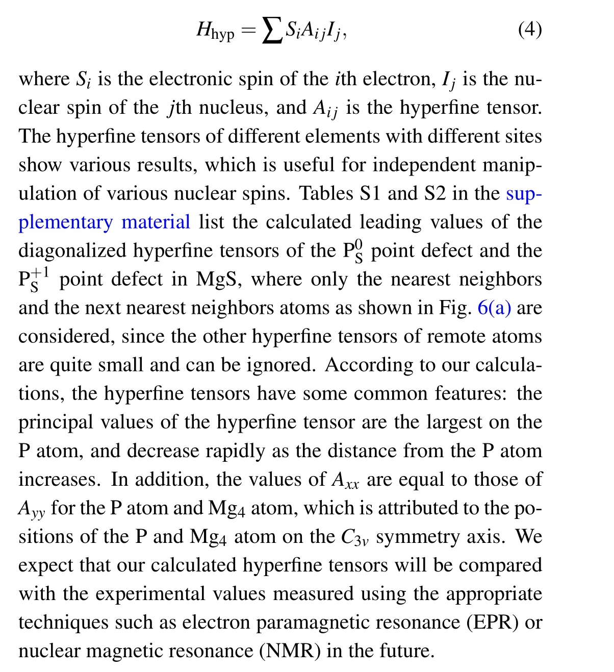
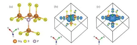
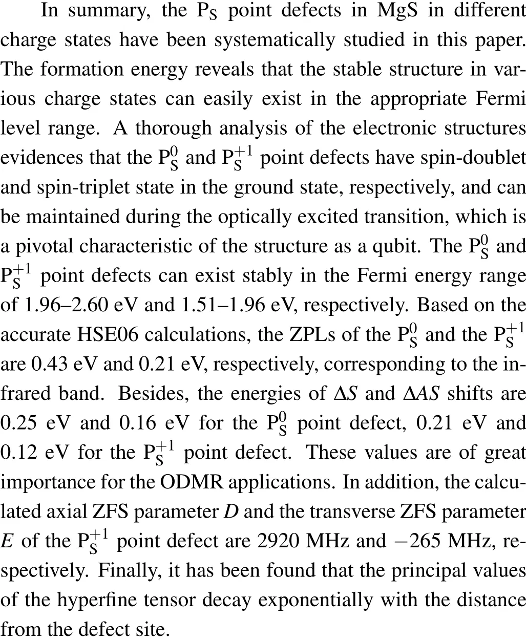
Fig.6. Schematic diagram of the local structure(a),the spin difference charge density of the P0S point defect(b)and the P+1S point defect(c)in MgS.We only show the atoms up to the second neighbors from the P atom,the isosurface value is 5×10⁻⁴ e/˚A3 for the spin difference charge density. The blue and green represent positive and negative,respectively.

Acknowledgements
Project supported by the National Natural Science Foundation of China (Grant No. 12164020) and the Natural Science Foundation of Jiangxi Province, China (Grant No. 20202BAB201012). We gratefully acknowledge Hefei Advanced Computing Center for computational support.